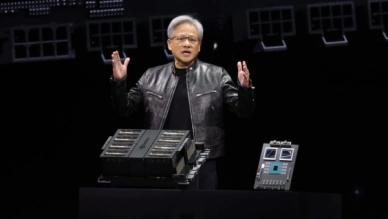
NVIDIA, the giant in the graphics chip industry, has just introduced its latest GPU architecture - Blackwell. This is considered a significant leap forward in the chip industry, promising breakthroughs in performance and unlocking new possibilities for AI and graphics applications. The standout feature of Blackwell is its unique Multi-Chip Module (MCM) design, which allows for the integration of two GPUs on a single chip, creating an unprecedentedly powerful computing machine.
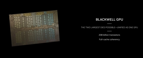
The Blackwell B200 GPU features a total of 208 billion transistors and is built using the 4NP TSMC process designed by NVIDIA. This design allows for the connection of two GPU chips on a single chip. Moreover, Blackwell employs the second generation of the Transformer Engine, doubling the computational workload with 4-bit AI inference capabilities.
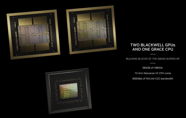
Notably, NVIDIA's fifth-generation NVLink provides bidirectional data transfer speeds of up to 1.8 TB/s per GPU, enhancing performance for complex AI models. The Blackwell B200 also integrates a RAS Engine, a tool that predicts and addresses issues, ensuring continuous operation and reducing operational costs for large-scale AI systems.
Additionally, the Blackwell B200 offers superior security features to protect AI models and data, along with a dedicated decompression engine for rapid data processing.
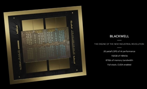
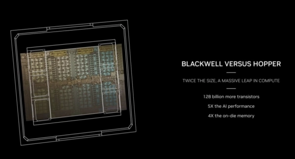
Compared to the Hopper GPU, the Blackwell B200 GPU boasts 128 billion more transistors, five times the AI performance with 20 petaFlops per chip, and four times the integrated memory. Furthermore, this GPU is paired with 8 HBM3e stacks, offering the world's fastest memory with a data transfer rate of 8 TB/s and up to 192 GB of HBM3e memory.
The NVIDIA Blackwell B200 GPU is one of two Blackwell chips used in various designs. It is the first NVIDIA GPU to utilize a new type of design called a chiplet (MCM), which consists of two computing chips. The chiplet design allows NVIDIA to enhance performance and reduce manufacturing costs, marking an important step in NVIDIA's technological advancement.
The Blackwell B200 is truly a "monster" GPU with a total of 160 SMs for 20,480 cores. The GPU utilizes advanced NVLINK connection technology, supporting 8 GPU architecture and 400 GbE network switches. However, this GPU will also consume significant power, with a maximum TDP of 700 W, similar to the H100 and H200 chips.
In terms of memory, the Blackwell B200 GPU features up to 192 GB of HBM3e memory, divided into eight stacks, each with 24 GB of VRAM and a bus interface of up to 8192-bit. This provides 2.4 times the memory capacity compared to the H100 80 GB GPU, allowing the chip to handle much larger datasets.
The NVIDIA Blackwell B200 GPU and its corresponding platforms will mark a new era in AI computing and create fierce competition with AMD and Intel's latest chips, which have yet to be widely adopted. The launch of Blackwell reaffirms NVIDIA's dominance in the AI market.
With its groundbreaking MCM architecture and superior AI performance, NVIDIA Blackwell is not just a new technology product but also a significant milestone in the history of GPU development. Blackwell promises to drive advancements in many fields, from artificial intelligence to 3D graphics, and open new doors for the future of technology. What do you think about the configuration and performance of the NVIDIA Blackwell B200 GPU?

Ngoc Phuong
Web Developer
Thank you for visiting my website. My name is Ngoc Phuong, and I have over 10 years of experience in website development. I am confident in stating that I am an expert in creating impressive and effective websites. If you need a website designed, please feel free to contact me via email at [email protected].
Submit feedback
Your email address will not be made public. Fields marked are required *
Search
Trend
-

What is Black Myth: Wukong? Detailed Guide on System Requirements and Gameplay
08-21-2024 . 1k view
-

The simplest and fastest way to log into the Chinese TikTok, Douyin.
01-10-2022 . 1k view
-

Blog sites that will accept AI generated content
07-26-2024 . 1k view
-

Call of Duty: Black Ops 6 - Intense, Mysterious, and Surprising Warfare
09-02-2024 . 1k view
-
The "End of Life" for Windows 10: A Massive E-Waste Threat and Sustainable Solutions
08-18-2024 . 951 view


0 feedback